HOME

Tuesday, August 16, 2011

Nanotechnology – the new threat to food

Following on from genetic engineering, nanotechnology represents the latest high technology attempt to infiltrate our food supply. Senior scientists have warned that nanotechnology, the manipulation of matter at the scale of atoms and molecules, introduces serious new risks to human and environmental health. Yet in the absence of public debate, or oversight from regulators, unlabelled foods manufactured using nanotechnology have begun to appear on our supermarket shelves.

Around the world there is an increase in interest in our food, health and environment. Where are products produced, how, why, by whom, how far have they travelled, how long have they been stored etc. The organic and local food movements have emerged as an intuitive and practical response to the increasing use of chemicals in food production, and to the growing alienation of industrial agribusiness from holistic agricultural systems. People have chosen to eat organic foods because they care about the health of their families and the health of the environment. Organic agriculture also enables people to support integrated, environmentally friendly agriculture, and appropriate technology, rather than chemical-intensive factory farming.

Support for organics has also grown as a direct response to biotechnology giants’ efforts to genetically engineer our food crops. Farmers and food buyers around the world were, and continue to be, enraged by the introduction of genetically engineered food crops. For many, the inevitable conclusion was that whereas the biotechnology companies stood to benefit from the entry of genetically engineered foods into the food chain, consumers, farmers and the environment shouldered all the risks.

Now, nanotechnology introduces a new wave of assaults on our foods. Nanotechnology is the high technology, atomically processed antithesis to organic agriculture, which values the natural health-giving properties of fresh, unprocessed wholefoods. It further transforms the farm into an automated extension of the high technology factory production line, using patented products that will inevitably concentrate corporate control. It also introduces serious new risks for human health and the environment.

Introduction to nanotechnology – what is it, why is it different

Nanotechnology is a powerful new technology for taking apart and reconstructing nature at the atomic and molecular level. Nanotechnology embodies the dream that scientists can remake the world from the atom up, using atomic level manipulation to transform and construct a wide range of new materials, devices, living organisms and technological systems.

Nanotechnology and nanoscience involve the study of phenomena and materials, and the manipulation of structures, devices and systems that exist at the nanoscale, <100 nanometres (nm) in size. To put 100nm in context: a strand of DNA is 2.5nm wide, a protein molecule is 5nm, a red blood cell 7,000 nm and a human hair is 80, 000 nm wide.

The properties of nanoparticles are not governed by the same physical laws as larger particles, but by quantum mechanics. The physical and chemical properties of nanoparticles – for example, colour, solubility, strength, chemical reactivity and toxicity - can therefore be quite different from those of larger particles of the same substance.

The altered properties of nanoparticles have created the possibility for many new profitable products and applications. Engineered nanoparticles are used in literally hundreds of products that are already available on supermarket shelves – including transparent sunscreens, light-diffracting cosmetics, penetration enhanced moisturisers, stain and odour repellent fabrics, dirt repellent coatings, long lasting paints and furniture varnishes, and even some food products.

The Asia Pacific Economic Cooperation (APEC) Centre for Technology Foresight has predicted that nanotechnology will revolutionise all aspects of our economy and all aspects of society, with associated large-scale social upheaval.

How will nanotechnology be used for food production and processing?

Industry analysts and proponents predict that nanotechnology will be used to transform food from the atom up: “Thanks to nanotechnology, tomorrow’s food will be designed by shaping molecules and atoms. Food will be wrapped in “smart” safety packaging that can detect spoilage or harmful contaminants. Future products will enhance and adjust their color, flavor, or nutrient content to accommodate each consumer’s taste or health needs. And in agriculture, nanotechnology promises to reduce pesticide use, improve plant and animal breeding, and create new nano-bioindustrial products” – or so states the US Project on Emerging Nanotechnologies’ recent report on the use of nanotechnology in food and agriculture (available at http://www.nanotechproject.org).

The food and agriculture industries have been investing billions of dollars into nanotechnology research, with an unknown number of unlabeled nano food products already on the market. In the absence of mandatory product labelling anywhere in the world, it is impossible to tell how many commercial food products now contain nano ingredients. The Helmut Kaiser Consultancy Group, a pro-nanotechnology analyst, suggests that there are now over 300 nano food products available on the market worldwide. It estimates that the global nano food market was worth US$5.3 billion in 2005 and will rise to US$20.4 billion by 2010. It predicts that nanotechnology will be used in 40% of the food industries by 2015.

There are four key focus areas for nanotechnology food research:
• Nano-modification of seed and fertilisers/ pesticides
• Food ‘fortification’ and modification
• Interactive ‘smart’ food
• ‘Smart’ packaging and food tracking

Nano-modification of seed and fertilisers/ pesticides

Proponents say that nanotechnology will be used to further automate the modern agribusiness unit. All farm inputs – seeds, fertilisers, pesticides and labour – will become increasingly technologically modified. Nanotechnology will take the genetic engineering of agriculture to the next level down – atomic engineering. Atomic engineering could enable the DNA of seeds to be rearranged in order to obtain different plant properties including colour, growth season, yield etc. Highly potent atomically engineered fertilisers and pesticides will be used to maintain plant growth. Nano-sensors will enable plant growth, pH levels, the presence of nutrients, moisture, pests or disease to be monitored from far away, significantly reducing the need for on-farm labour inputs. The concerned organisation, The Action Group on Erosion, Technology and Concentration (ETC) warns in its seminal report “Down on the Farm” (available at http://www.etcgroup.org), in a nanotechnology shaped future, “the farm will be a wide area biofactory that can be monitored and managed from a laptop and food will be crafted from designer substances delivering nutrients efficiently to the body”.

Food ‘fortification’ and modification

Nanotech companies are working to fortify processed food with nano-encapsulated nutrients, its appearance and taste boosted by nano-developed colours, its fat and sugar content removed or disabled by nano-modification, and ‘mouth feel’ improved. Food ‘fortification’ will be used to increase the nutritional claims that can be made about a given processed food – for example the inclusion of ‘medically beneficial’ nano-capsules will soon enable chocolate chip cookies or hot chips to be marketed as health promoting or artery cleansing. Nanotechnology will also enable junk foods like ice cream and chocolate to be modified to reduce the amount of fats and sugars that the body can absorb. This could happen either by replacing some of the fats and sugars with other substances, or by using nanoparticles to prevent the body from digesting or absorbing these components of the food. In this way, the nano industry could market vitamin and fibre-fortified, fat and sugar-blocked junk food as health promoting and weight reducing.

Interactive ‘smart’ food

Companies such as Kraft and NestlĂ© are designing ‘smart’ foods that will interact with consumers to ‘personalise’ food, changing colour, flavour or nutrients on demand. Kraft is developing a clear tasteless drink that contains hundreds of flavours in latent nanocapsules. A domestic microwave could be used to trigger release of the colour, flavour, concentration and texture of the individual’s choice. ‘Smart’ foods could also sense when an individual was allergic to a food’s ingredients, and block the offending ingredient. Or alternatively, ‘smart’ packaging could release a dose of additional nutrients to those which it identifies as having special dietary needs, for example calcium molecules to people suffering from osteoporosis.

‘Smart’ packaging and food tracking

Nanotechnology will dramatically extend food shelf life. Mars Inc. already has a patent on an invisible, edible, nano wrapper which will envelope foods, preventing gas and moisture exchange. ‘Smart’ packaging (containing nano-sensors and anti-microbial activators) is being developed that will be capable of detecting food spoilage and releasing nano-anti-microbes to extend food shelf life, enabling supermarkets to keep food for even greater periods before its sale. Nano-sensors, embedded into food products as tiny chips that were invisible to the human eye, would also act as electronic barcodes. They would emit a signal that would allow food, including fresh food, to be tracked from paddock to factory to supermarket and beyond.

What are the key concerns about nanotechnology in food and agriculture?

Concerns about the use of nanotechnology in agriculture and food production relate to the further automation and alienation of food production, serious new toxicity risks for humans and the environment, and the further loss of privacy as nano surveillance tracks each step in the food chain. The failure of governments to introduce laws to protect the public and the environment from nanotechnology’s risks is a most serious concern.

Nanotechnology in agriculture is based on the premise that we can improve efficiency and productivity by rearranging atoms in seeds, by developing even more potent chemical inputs, by using high technology surveillance to allow electronic, rather than person-based surveillance of on-farm conditions, and by further automating inputs to plant growth. Applications of nanotechnology to food processing assume that humans can ‘improve’ the taste, texture, appearance, nutritional content and longevity of food by manipulating it at the atomic level. It has even been argued that this will result in food that is ‘safer’.

These assumptions are based on a flawed belief that humans can remake the natural world from the atom up – and get a better result. It assumes that we can predict the consequences of our actions, even when we are dealing with highly unpredictable processes and forces – such as quantum mechanics. Unfortunately, history tells us that we are simply not very good at predicting the outcomes of complex systems – witness the disasters that resulted from the introduction of biological controls such as the Cane Toad, or the introduction of rabbits and foxes for sport. History is similarly littered with examples of huge health and environmental problems that resulted from the failure to respond to early warning signs about previous perceived “wonder” materials such as CFCs, DDT and asbestos. This suggests that we should take the early warning signs associated with the toxicity of nanoparticles very seriously.

There is a small but growing body of toxicological literature that suggests that nanoparticles are more reactive, more mobile, and more likely than larger particles to be toxic to humans and the environment. Preliminary scientific research has shown that many types of nanoparticles can result in increased oxidative stress which can result in the formation of free radicals that can lead to cancer, DNA mutation and even cell death. Fullerenes, carbon nanoparticles, have been found to cause brain damage in largemouth bass, a species accepted by regulatory agencies as a model for defining ecotoxicological effects.

In its 2004 report, the United Kingdom’s Royal Society recognised the serious risks of nanotoxicity and recommended that “ingredients in the form of nanoparticles should undergo a full safety assessment by the relevant scientific advisory body before they are permitted for use in products”. Despite this warning, two years after the Royal Society’s report, there are still no laws governing the use of nanomaterials in consumer products to ensure that they do not cause harm to the public using them, the workers producing them, or the environmental systems in which waste nanoproducts are released.

The use of nano-surveillance in food packaging will also introduce new privacy concerns. As the food industry’s use of nano-tracking increases, it will gain the capacity to track the movement of food from the paddock, to the factory, to the supermarket and to your dinner plate. This will raise serious new privacy issues for which we are poorly prepared.

Alarmingly, despite the release into supermarkets and into the environment of nano food and agriculture products, governments world wide have yet to introduce any regulation to manage nanotechnology’s risks.

The struggle for a healthy food future - what are the alternatives to nanotechnology?

What will our food and technological future look like? We are in an epic battle for control of our food supply. Corporate or community ownership, global or local, small versus massive, processed versus wholesome. These are the paradigms that we need to choose between. A key way to promote healthy, holistic agriculture is to support it with our purchasing choices. Certified organic foods offer you better health, a better environment and a way for you to support a nano-free food future. With personal care products, buy organic or from a company that states they do not use nanotechnology.

There are many ways to help create a healthy food future. Shop at a farmers market or buy from a box scheme direct from a farmer, buy from an organic store or from the organic section in a supermarket. Consider joining a community garden, or starting a garden of your own. Start an organic kitchen garden at your pre school or school. Read product labels, get involved and interested. Talk to your friends and family about the food issues that matter most to you. Let companies know through their 1800 feedback lines that you are concerned about the use of nanotechnology in their products. Tell your local member of parliament that you want to see products that contain engineered nano ingredients labelled to allow you to make an informed purchasing choice.

It is exciting to see food politics debated by our mainstream media and our research and education institutions. However while there are already unlabelled food products that contain engineered nano ingredients available in our supermarkets, nanotechnology is only just starting to gain some attention. There are no regulations in place to protect public and environmental health, and almost no corporate or public monies being spent looking at the long-term consequences of manipulating our food at the atomic level. The similarity to the introduction of genetic engineering with the added risk that there is no regulatory oversight is chilling.

We must all get politically active on nanotechnology just as we did with genetic engineering. It is essential that we get moratoria enacted on the use of nanotechnology until we have regulatory systems in place to protect human and environmental health, and until we have genuine public involvement in decision making regarding nanotechnology’s introduction. We must also ensure our Governments put our hard-earned taxpayer dollars into support for the organic sector.

Together, we can create a healthy food future that delivers to our community not corporate profits.

Nanotechnology (general)

In layman's terms, nanotechnology refers to materials, applications and processes designed to work on extremely tiny scales. A nanometre is one-billionth of a metre. A sheet of paper is about 100,000 nanometres thick, while a single gold atom is about one-third of a nanometre in diameter.

Many unique properties and uses can be derived from structures built at the nanoscale, giving nanotechnology enormous potential for future development.

A relatively new and emerging field of science, nanotechnology was first alluded to in 1959, but remained largely theoretical until the 1980s. The invention of the scanning tunneling microscope (STM) allowed the first direct manipulation of individual atoms.

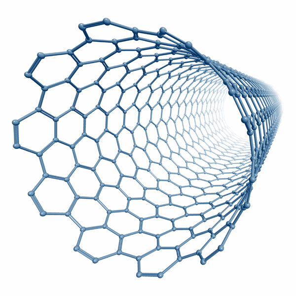
Carbon nanotubes were demonstrated in 1991. These cylindrical structures were found to possess exceedingly high strength and unique electrical properties, as well as being highly efficient thermal conductors.


Various other structures were developed over the following two decades, each built on an atom-by-atom basis.

Today, nanotechnology is among the fastest growing areas of science and technology, with exponential progress being made. Just some of the recent breakthroughs have included:

The first integrated circuits using three-dimensional carbon nanotubes. These could be vital in maintaining the growth of computer power, allowing Moore's Law to continue.

Solar panels with greater efficiency through the use of nanotechnology materials.

Water purification bottles, with filters only 15 nanometres in width, allowing military personnel and also civilians hit by disasters to create safe drinking water (even if that water comes from a filthy source).

Military equipment made lighter and stronger through the use of nanomaterial composites.

Nanostructured polymers in display technologies allowing brighter images, lighter weight, less power consumption and wider viewing angles.

Nanotechnology surfaces which are highly resistant to bacteria, dirt and scratches.

New fabrics that are highly resistant to liquid, causing it to simply fall off without leaving any dampness or stains.

Nanostructured catalysts used to make chemical manufacturing processes more efficient, saving energy and reducing waste products.

Pharmaceutical products reformulated with nanosized particles to improve their absorption and make them easier to administer.

There are many other applications and the list is growing all the time. By 2025, nanotechnology is expected to be a mature industry, with countless mainstream products.


Further into the future, nanotechnology will play a major role in medicine and longevity. Blood cell-sized devices will go directly into the human body, eradicating pathogens and keeping people healthy. Full-immersion virtual reality and other advanced concepts will become possible through the use of these "nanobots".

Meanwhile, so-called "nanofabricators" would allow the creation of macro-scale objects on an atom-by-atom basis. Home appliances using this technology could serve as 3-D printers - downloading products from the web and literally building them from scratch. Physical items would each have their own code or algorithm that would program the machine to create them.

Quantum computers, invisibility cloaks and space elevators may one day become a reality, thanks to nanotech.

In the more distant future, nanotechnology could allow humans to make the transition to fully non-biological forms. Entire bodies and brains could be reconstructed at the atomic scale, leading to practical immortality.

Much debate has taken place on the implications of nanotechnology. It has the potential to create radically new materials and devices with a vast range of applications in engineering, medicine, electronics and energy production. On the other hand, nanotechnology raises many of the same issues as with any introduction of new technology - including concerns about the toxicity and environmental impact of nanomaterials, and their potential effects on global economics, as well as speculation about various doomsday scenarios. These concerns have led to a debate among advocacy groups and governments on whether special regulation of nanotechnology is required.


Electrical Engineering and relation on Nanotechnology

1. INTRODUCTION

Nanotechnology has affected nearly every field of Engineering and Science but most of the innovation and funding (private) in Nanotechnology came from Electronics giants, in search for making faster computers. The other fields that worked with nano electronics hand in hand were nano-photonics and nano-instrumentation. Also the marketing and making of nano gadgets started from the computers and mobiles which are the only machines made at nano scale that were available economically in the market at a very early stage. So it is of no doubt that the only area where nanotechnology penetrated deeply is electronics where it had lead to cost advantage and performance attributes especially in transistors and today we have 1 billion transistors in the latest processor. The backbone of nanotechnology in electronics are the results that we have taken from nano physics that is quantum physics and solid state physics because then we talk of things at nano scale these are the two stream of physics that helps us in predicting things. Eventually when we talk of electronics it is all about electrons and how we use them in various gadgets to get the required result. So it is very important to know electrons and how it behaves at nano scale in electronics.

Introduction and Importance Quantum Mechanics A fundamental aspect of quantum mechanics is the particle-wave duality, introduced by De Broglie, according to which any particle can be associated with a matter wave whose wavelength is inversely proportional to the particle's linear momentum. Whenever the size of a physical system becomes comparable to the wavelength of the particles that interact with such a system, the behavior of the particles is best described by the rules of quantum mechanics. All the information we need about the particle is obtained by solving its Schrodinger equation. The solutions of this equation represent the possible physical states in which the system can be found. But quantum mechanics is not required to describe the movement of objects in the macroscopic world. The wavelength associated with a macroscopic object is in fact much smaller than the object's size, and therefore the trajectory of such an object can be excellently derived using the principles of classical mechanics. Things change, for instance, in the case of electrons orbiting around a nucleus, since their associated wavelength is of the same order of magnitude as the electron-nucleus distance. We can use the concept of particle-wave duality to give a simple explanation of the behavior of carriers in a semiconductor nanocrystal. In a bulk inorganic semiconductor, conduction band electrons (and valence band holes) are free to move throughout the crystal, and their motion can be described satisfactorily by a linear combination of plane waves whose wavelength is generally of the order of nano-meters. This means that, whenever the size of a semiconductor solid becomes comparable to these wavelengths, a free carrier confined in this structure will behave as a particle in a potential box. The solutions of the Schrodinger equation in such case are standing waves confined in the potential well, and the energies associated with two distinct wave functions are, in general, different and discontinuous. This means that the particle energies cannot take on any arbitrary value, and the system exhibits a discrete energy level spectrum. Transitions between any two levels are seen as discrete peaks in the optical spectra, for instance. The system is then also referred to as ''quantum confined''. The main point here is that in order to rationalize (or predict) the physical properties of nanoscale materials, such as their electrical and thermal conductivity or their absorption and emission spectra, we need first to determine their energy level structure.

2. THEORY OF NANO-ELECTRONICS

2.1 PRESENT STATE OF NANO-ELECTRONICS. Moore's law states that the number transistor on an integrated chip for a component doubles every two years. How ever this law does not holds perfectly true for RAM (Random Access memory). This does not mean that the number of transistor on a chip increases but about the density of transistors at which the cost per transistor is the lowest.Currently processors are fabricated at 90nm and 65nm that are being introduced by Intel. The 90 nanometer (90 nm) process refers to the level of semiconductor process or fabrication technology that wasachieved in the 2002-2003 period, by most leading semiconductor companies, like Intel, Texas Instruments, IBM etc. However it is not true for RAM and hard disk. New materials seeing possible use in nano-electronics and will probably keep this law on track. The future is seen as molecular electronics but there is lots of work still to be done to make that possible.

2.2 SILICON NANOTECHNOLOGY
2.2.1 CMOS Nanotechnology

For the past several decades, miniaturization in silicon integrated circuits has pro- gressed steadily with an exponential scale described by Moore's Law. This incredible progress has generally meant that critical dimensions are reduced by a factor of two every three years, while chip density increases by a factor of four over this period. However, modern chip manufacturers have been accelerating this pace recently, and currently chips are being made with gate lengths in the 45 to 65 nm range. More scaling is expected, however, and 15-nm gate lengths are scheduled for production before the end of this decade.

In MOSFET there is electric field between the gate and the semiconductor is such that an inverted carrier population is created and forms a conducting channel. This channel extends between the source and drain regions, and the transport through this channel is modulated by the gate potential. As the channel length has gotten smaller, there has been considerable effort to incorporate a variety of new effects into the simple (as well as the more complex) models. These include short-channel effects, narrow width effects, degradation of the mobility due to surface scattering, hot carrier effects, and velocity overshoot. Ballistic transport in the MOSFET (discussed in later part) Thermodynamics is just as significant in limiting scaling as the preceding effects. The first way it limits scaling is in its control of the subthreshold behavior of MOSFETs. The subthreshold current of a MOSFET originates in the high-energy tail of the statistical distribution of carriers in its source region. The carriers in the source are governed by Fermi-Dirac statistics, and so the tail of the distribution is essentially Boltzmann.
There two major scattering regions - the barrier between the channel and the source and within the channel.

There also exists a phenomenon Granularity is the failure of thermodynamic averaging in small devices. Quantum behavior in the device, there are two effects and Effective Carrier Wave Packet . These effects also include tunneling through the gate insulator, tunneling through the band gap, quantum confinement issues, interface scattering, discrete atomistic effects in the doping and at interfaces, and thermal problems associated with very high power densities.
Ballistic Properties:-
It is the phenomenon where the the contribution in electrical resistivity due to scattering by the atoms, molecules or impurities in the medium itself, is negligible or absent meaning the electron can move without hindrances. There is no loss of kinetic energy due to collision of hitting of electrons with atom of metal thereby electrons move in a mean free path where it can move freely.

Quantum mechanical scaling limitations include both confinement effects and tun- neling effects. Confinement effects occur when electron or hole wave functions are squeezed into narrow spaces between barriers. In FETs this primarily happens in the channel, where the charges are squeezed between the gate insulator on one side and the built-in field of the body on the other side. Quantum confinement in this approximately triangular well raises the ground state energy of the electrons or holes, which increases the threshold voltage, and shifts the mean position of the carriers a little farther from the Si-SiO2 interface. Quantum mechanical tunneling is generally more detrimental to scaling than the Confinement effects. When electrons or holes tunnel through the barriers of the FET, it causes leakage current. As scaling continues, this ultimately causes unacceptable increases in power dissipation. The leakage may also cause some types of dynamic logic circuits to lose their logic state, but the former problem usually seems to arise first.

There are primarily two forms of tunneling leakage: tunneling current through the gate insulator, and tunneling current through the drain-to-body junction. The atomistic effects that cause limitations to scaling are those in which the discreteness of matter gives rise to large statistical variations in small devices. These statistical variations occur because the atoms or molecules tend to display Poisson statistics in their number or position, and the Poisson distribution for small numbers can become very wide.
2.2.2 Memory
As the semiconductor device feature size enters the sub-50-nm range, two new effects come into play. One is the quantum effect, which is rooted in the wave nature of the charge carriers, and gives rise to non classical transport effects such as resonant tunneling and quantum interference. The other is related to the quantized nature of the electronic charge, often manifested in the so-called single-electron effect: Charging each electron to a small confined region requires a certain amount of energy in order to overcome the Coulomb repulsion; if this charging energy is greater than the thermal energy, kb*T (kb Boltzman constant, T temperature), a single electron added to the region could have a significant effect on other electrons entering the confined region.

To increase the storage density of semiconductor memories, the size of each memory cell must be reduced. A smaller memory cell also leads to higher speed and lower power consumption. This is the incentive for studying the nanoscale semiconductor memory. One of the general schemes for semiconductor data storage is by storing charges on a capacitor. The charged state and the uncharged state can be used to represent binary information 1 and 0, respectively. Usually charges are transferred to the capacitor through a resistive. The motivation for this work is to investigate the ultimate limit of a floating gate MOS memory. In a conventional floating gate memory, there are typically on the order of 10 to power 4 electrons stored on the floating gate to represent one bit of information. The ultimate limit in scaling down the floating gate memory is to use only one electron for the same purpose, hence the name "single-electron MOS memory" (SEMM). The advantage of such a memory is that not only can it be very small, but also it can provide some unique characteristics that are not available in the conventional device, such characteristics as quantized threshold voltage shift and quantized charging voltage.

To make single-electron memory practical, both thermal fluctuation and quantum fluctuations of the stored charge have to be minimized. In order to reduce the variation in the device structure, we would like to build a single-electron memory device in crystalline silicon that has well-controlled dimensions. We defined the transistor channel and the floating gate by using lithography. Finally, the single-electron memory potentially has a number of advantages over conventional memories: (1) the quantized characteristics of the device make it immune to the noise from the environment-unless the noise level reaches a certain threshold, it will not affect the memory state. The immunity to noise is especially important for the future terabits integration, simply because of the sheer large number of devices present on a single small chip area. (2) the inherent quantized nature of the SEMM makes it possible to easily implement multilevel logic storage in a single memory cell; (3) the device can operate at a higher speed due to the use of only one or few electrons during writing and erasing; (4) for the same reason, the device can also have ultralow power consumption.

2.3 NANO TUBES, CNT ELECTRONICS.
Single-walled carbon nanotubes (SWNTs), which are graphite cylinders made of a hexagonal carbon-atom lattice, have drawn a great deal of interests due to their Fundamental research importance and tremendous potential technical applications . For Example, they might play an important role in future molecular electronic devices, such as room-temperature single electron and field-effect transistors , and rectifiers . A SWNT can be either a semiconductor or a metal, depending on its helicity and diameter. The electronic properties of the SWNT have been the subject of an increasing number of experimental and theoretical studies since 1995. And it is expected that very soon SWNT will see it's application in Nano electronics. SWNT is going to see it's application in transistors where it can reduce the gate length and also reduce leakage current. SWNTs have very low electrical resistance. Resistance occurs when an electron get deflected away from its path, when it is traveling through a material. In a 3-D conductor, electrons have plenty of opportunity to scatter, since they can do so at any angle. All these scatterings will give rise to electrical resistance. The situation is different in 1D. In a truly 1D conductor, however, electrons can only travel forward or backward. Only backscattering will lead to electrical resistance. But backscattering in nanotubes is impeded by the special symmetry of graphite and carbon nanotubes, and is therefore less likely to happen. Because of this, electrons can travel in nanotubes for long distances without being scattered, and this type of ballistic transport has been observed experimentally

2.4 NANO WIRES

A nanowire is a wire of dimensions of the order of a nanometer. They are also called quantum wires because their properties are governed by quantum mechanics. They can be used to link or connect tiny component is nanocircuits. They are referred as 1 dimensional materials (because their length to width ratio is very high). The electrons here are quantum confined and occupy different energy levels than those of bulk material. They will see their application in electronics, opto-electronics and Micro Electro mechanical systems. They will be seeing possible applations in future molecular electronic devices, as resonant tunneling diodes, single-electron transistors, and field effect structures and also in making logic gates.

2.5 QUANTUM DOT

It is the semiconductor nanostructure which exhibits the phenomenon of confining motions of electrons of conduction, valence or excitons in all three spatial directions. They have superior quantum and optical properties and are being researched for diode laser, amplifier, sensors, etc. They are also seeing application in Light Emitting Diodes(Quantum Dot Single Electron Device). The ability to control electron charging of a capacitive node by individual electron makes there devices suitable for memory application. A quantum well is a potential well that confines particles, which were originally free to move in three dimensions, to two dimensions, forcing them to occupy a planar region.

3. MANUFACTURING CHALLENGES Nanofabrication is being developed to construct devices such as resonant tunneling diodes and transistors and single electron transistors and carbon nanotube transistors. The most common type of transistor being developed for use at the nanoscale is the field effect transistor. Economics issues are constraining nano-electronics to hit market. Two ways of manufacturing nano materials are:-

1. Bottom up self assembly (wet chemistry) In this type of fabrication we start from atoms or molecules to get to the desired material.
2. Top down self assembly (Lithography and derivatives) In this type of fabrication the bulk material is broken down into smaller pieces. Thought we have knowledge about many new materials and their physics at nanoscale but to get the technology economically available (cost effective) and to get the state of art levels of manufacturing nanomaterials is still under development.

Nanotechnology - Future uses

It is difficult to predict when exactly nanotechnology assemblers or assembly stations will be operational to make nanotechnology a worldwide commercial reality. However here are a few potential results of the use of nanotechnology:

The replication of anything including water and food completely eliminating famine and poverty because production costs of nearly all products - including food - will drop to near-zero.

In the information technology industry, the smallest size of transistors on silicon microprocessors is about to reach it's limit. Moore's Law predicts that by about 2015 we must be working at the molecular level to advance. Nanotechnology will enable the development of a new generation of smaller more powerful components. In fact one of the specific goals of the U.S. government's nanotechnology initiative is to develop a memory device approximately the size of a sugar cube capable of storing all the information in the U.S. national library. PCs with comparable speeds of current equipment will be the size of a grain of sand and will be capable of operating for decades on one small battery. So effectively nanotechnology will make computers disappear; they will be in our bodies, clothing, refrigerators, buildings, absolutely everywhere. As materials will be engineered on the molecular scale they will incorporate computation in the same way that certain materials have a specific colour. Within the next 25 years scientists will have reverse-engineered the physical processes in the human brain that result in thought, which will lead to biologically inspired computer software (artificial intelligence) enabling materials to "think" for themselves.

In the medical industry, medicines could contain nanorobots programmed to destroy the molecular structure of cancer cells and viruses. Nanorobots could be used by surgeons to change your physical appearance or perform operations without leaving a scar. It may even be possible that nanorobots could slow or reverse the aging process. Nanotechnology and biotechnology will be combined to create ingestable systems that will be able to tell medics the location of diseased cells and the type of disease. At some point disease and genetic defects will be eliminated through the alteration of the body at the atomic level, effectively re-coding your DNA.

Environmentally friendly airborne nanorobots could be programmed to rebuild the ozone layer atom by atom. Water sources could be purified saving millions of lives and oil spillages could be removed quickly and completely. The dependence on the Earth's natural resources for our energy would also be eliminated and pollution would be a thing of the past because pollutants can be reduced to their component atoms and recycled.

For the hearing impaired nanotechnology machines will use advanced speech recognition to create subtitles automatically and on the fly. Blind people will have reading machines that could be incorporated into clothing that would use advanced text recognition allowing the user to read signs, menus, displays etc. Smilar nanotechnology devices will also be used to translate text information from one language to another.

Virtual reality will become much more life-like, glasses will be able to display images directly onto our retinas and contact lenses will allow full-immersion virtual reality.

The house of the future will use nanotechnology to be able to change colour to whatever you decide and generate more electricity than it consumes.
Aerospace and automotive materials will change substantially. Currently aluminium, nickel, and titanium alloys and carbon fibre composites are used but in the future materials made of lightweight, high-strength carbon nanotubes will be used. Carbon nanotubes are the world's strongest material in terms of tensile strength and they are lightweight and flexible. This will result in aircraft and cars being 100 times lighter and therefore would be much more fuel efficient. As the graphite (the carbon allotrope in the nanotubes) has a network of hexagonal rings it has many unpaired electrons. Therefore carbon nanotubes conduct electricity and heat amazingly well and are being considered for use as wires for nanosized electronic devices in future computers, charge-storage devices in batteries, and electron guns for semiconductor chip etching and flat-screen televisions and computer monitors. They also could store hydrogen gas to power fuel cells. Thus, there is intense interest in finding a way to produce nanotubes in large quantities.

Top 10 Uses of NanoTechnology in Food

Nanoparticles may be able to detect bacteria, extend food shelf life, add health benefits, or improve flavor, reports Discovery.

While nanotechnology does not involve any genetic manipulation, many companies are keeping secret about their work their doing. While this can keep competitors off their trail, it can also make it difficult for regulatory agencies to manage risks and create laws for these emerging technologies.

Nonetheless, nanotechnology offers some exciting potential benefits for the quality and safety of our foods.

1. CONTAMINATION SENSOR: Flash a light to reveal the presence of E. coli bacteria.

2. ANTIMICROBIAL PACKAGING: Edible food films made with cinnamon or oregano oil, or nano particles of zinc, calcium other materials that kill bacteria.

3. IMPROVED FOOD STORAGE: Nano-enhanced barrier keeps oxygen-sensitive foods fresher.

4. ENHANCED NUTRIENT DELIVERY
Nano-encapsulating improves solubility of vitamins, antioxidants, healthy omega oils and other ‘nutraceuticals’.

5. GREEN PACKAGING: Nano-fibers made from lobster shells or organic corn are both antimicrobial and biodegradable.

6. PESTICIDE REDUCTION: A cloth saturated with nano fibers slowly releases pesticides, eliminating need for additional spraying and reducing chemical leakage into the water supply.

7. TRACKING, TRACING; BRAND PROTECTION: Nanobarcodes can be created to tag individual products and trace outbreaks.

8. TEXTURE: Food spreadability and stability improve with nano-sized crystals and lipids for better low-fat foods.

9. FLAVOR: Trick the tongue with bitter blockers or sweet and salty enhancers.

10. BACTERIA IDENTIFICATION AND ELIMINATION: Nano carbohydrate particles bind with bacteria so they can be detected and eliminated.


Friday, April 15, 2011

Nanotechnology – How it can be a Boon for curing critical ailments

Gone are the days when the term ‘Nanotechnology’ could only be seen if someone went through the pages of some sci-fi novel. This term has proved to be a boon to the human civilization with lots of offerings, the most significant one being in the field of medical science. It has proved to be very helpful in curing critical Medical Ailments and has shown prospects of further growth in the near future which may see a rise of around $60 billion worth of demand for nano-medicines within 1-2 years.

What exactly is Nanotechnology?

Now you may be wondering what this entire buzz about nanotechnology is and what exactly it is. Basically nanotechnology can be described as a completely new field and dimension in applied science which enables to develop nano bots and medicines at the microscopic level. In the medicinal field, this nanotechnology is being used to store critical information in nanometer sized chips which ultimately helps in detecting several critical diseases. You can have your disease cured even without the use of surgery, something which one couldn’t think about in the recent past.

How can nanotechnology be helpful in curing diseases?

It is worth noting that most of the diseases we come across our lifetime, are mere external manifestations of some disturbances in the molecular or the cellular level. Now, if the roots of the disease are cured and taken off from the cellular level itself, we won’t need to have complicated surgeries at the macro level. This utility of nanotechnology steers it to the forefront in curing several disease starting from any kind of eye ailments to even cancer. One can make use of the polymerized contact lenses developed by Nano engineers in Singapore, which helps in curing glaucoma by releasing small amounts of medicine. The alma mater of the fact is that, due to miniscule size of the nano bots or medicines, they can provide efficient Drug Delivery systems to the affected cells.

Nanotechnology for Cancer –The deadly disease:

It is well said that when MRI, PET or CT fails to detect the metastatic dormant cancer cells, Nanotechnology comes to use. Right from detecting the sources of this disease to finding an effective solution to cure it, nanotechnology does it all. Various researches being carried out throughout the world reveal that nanotechnology can be the ultimate answer to this disease. By detecting the vibration patterns of some high frequency ultrasounds, doctors can now differentiate cancer cells from normal cells. Unlike chemotherapy which kills both the normal as well as the cancer cells, nanotechnology researchers are currently in the process of making a device to kill only the cancer cells.

The Final Verdict:

If someone is still waiting for my final verdict on this huge arena of applies science, then the only thing I may suggest to you is to go and have a look at the various researches being carried out at the University of Pennsylvania, Cambridge University and other independent research firms and go through the results. The pace with which this field of applied and translational science is moving, it will surely eradicate some of the very critical ailments in the coming few years.

Nano News & Research


Researchers are working furiously to field defense nano technology for military application. Battle science laboritories are in hyperdrive to produce nanoscopic assemblers or nanogears to manipulate atomic matter and serve as replicators with endless production possibilities.

Nanobots and nano technology can be used to create innovative non woven textiles teeming with military potential. They offer promise as light weight ballistic protection, wound sealing properties, vitals tracking, and environmental adaptation to heating, cooling, and porous to non-porous membranes that can react to weather.


History

In the early 20th century, Henry Ford built a c
ar manufacturing plant on a 2,000-acre tract of land along the Rouge River in Michigan . Built to mass-produce automobiles more efficiently, the Rouge housed the equipment for developing each phase of a car, including blast furnaces , a steel mill and a glass plant. More than 90 miles of railroad track and conveyor belts kept Ford's car assembly line running. The Rouge model was lauded as the most efficient method of production at a time when bigger meant better.

The size of Ford's assembly plant would look strange to those born and raised in the 21st century.
In the next 50 years, machines will get increasingly smaller -- so small that thousands of these tiny machines would fit into the period at the end of this sentence. Within a few decades, we will use these nanomachines to manufacture consumer goods at the molecular level, piecing together one atom or molecule at a time to make baseballs, telephones and cars. This is the goal of nanotechnology . As televisions , airplanes and computers revolutionized the world in the last century, scientists claim that tactical nanotechnology will have an even more profound effect on the next century.

Nanotechnology is an umbrella term that covers many areas of research dealing with objects that are measured in nanometers . A nanometer (nm) is a billionth of a meter, or a millionth of a millimeter.

Building with Atoms
Atoms are the building blocks for all matter in our universe. You a
nd everything around you are made of atoms. Nature has perfected the science of manufacturing matter molecularly. For instance, our bodies are assembled in a specific manner from millions of living cells.
Cells are nature's nanomachines. Humans still have a lot to learn about the idea of constructing materials on such a
small scale. Consumer goods that we buy are made by pushing piles of atoms together in a bulky, imprecise manner. Imagine if we could manipulate each individual atom of an object. That's the basic idea of nanotechnology, and many scientists believe that we are only a few decades away from achieving it.
Nanogears no more than a nanometer wide could be used to construct a matter compiler, which could be fed
raw material to arrange atoms and build a macro-scale structure.


Nanotechnology is a hybrid science combining engineering and chemistry. Atoms and molecules stick together because they have complementary shapes that lock together, or charges that attract. Just like with magnets, a positively charged atom will stick to a negatively charged atom. As millions of these atoms are pieced together by nanomachines, a specific product will begin to take shape. The goal of nanotechnology is to manipulate atoms individually and place them in a pattern to produce a desired structure. There are three steps to achieving nanotechnology-produced goods:

Scientists must be able to manipulate individual atoms
. This means that they will have to develop a technique to grab single atoms and move them to desired positions. In 1990, IBM researchers showed that it is possible to manipulate single atoms. They positioned 35 xenon atoms on the surface of a nickel crystal, using an atomic force microscopy instrument. These positioned atoms spelled out the letters "IBM."

The next step will be to develop nanoscopic machines, called assemblers, that can be programmed to manipulate atoms and molecules at will. It would take thousands of years for a single assembler to produce any kind of material one atom at a time. Trillions of assemblers will be needed to develop products in a viable time frame.

In order to create enough assemblers to build

consumer goods, some nanomachines, called replicators , will be programmed to build more assemblers.

Trillions of assemblers and replicators will fill an area smaller than a cubic millimeter, and will still be too small for us to see with the naked eye . Assemblers and replicators will work together like hands to automatically construct products, and will eventually replace all traditional labor methods. This will vastly decrease manufacturing

costs, thereby making consumer goods plentiful, cheaper and stronger. In the next section, you'll find out how nanotechnology will impact every facet of society, from medicine to computers.

A New Industrial Revolution

In January 2000, U.S. President Bill Clinton requested a $227-million increase in the government's investment in nanotechnology research anddevelopment, which included a major initiative called the National Nanotechnology Initiative (NNI). This initiative nearly doubled America 's 2000 budget investment in nanotechnology, bringing the total invested in nanotechnology to $497 million for the 2001 national budget. In a written statement, White House officials said that "nanotechnology is the new frontier and its potential impact is compelling." About 70 percent of the new nanotechnology funding will go to university research efforts, which will help meet the demand for workers with nanoscale science and engineering skills. The initiative will also fund the projects of several governmental agencies, including the National Science Foundation , the Department of Defense , the Department of Energy , the National Institutes of Health , NASA and the National Institute of Standards and Technology. Much of the research will take more than 20 years to complete, but the process itself could touch off a new industrial revolution. Nanotechnology is likely to change the way almost everything, including medicine, computers and cars, are designed and constructed. Nanotechnology is anywhere from five to 15 years in the future, and we won't see dramatic changes in our world right away. But let's take a look at the potential effects of nanotechnology on military tactical gear:


The first products made from nanomachines will be stronger fibers. Eventually, we will be able to replicate anything, including diamonds , water and food. Famine could be eradicated by machines that fabricate foods to feed the hungry.

In the computer industry, the ability to shrink the size of transistors on silicon microprocessors will soon reach its limits. Nanotechnology will be needed to create a new generation of computer components. Molecular computers could contain storage devices capable of storing trillions of bytes of information in a structure the size of a sugar cube.


Nanotechnology may have its biggest impact on the medical industry. Patients will drink fluids containing nanorobots programmed to attack and reconstruct the molecular structure of cancer cells and viruses to make them harmless. There's even speculation that nanorobots could slow or reverse the aging process, and life expectancy could increase significantly. Nanorobots could also be programmed to perform delicate surgeries -- such nanosurgeons could work at a level a thousand times more precise than the sharpest scalpel. By working on such a small scale, a nanorobot could operate without leaving the scars that conventional surgery does. Additionally, nanorobots could change your physical appearance. They could be programmed to perform cosmetic surgery, rearranging your atoms to change your ears, nose, eye color or any other physical feature you wish to alter.

Nanotechnology has the potential to have a positive effect on the environment. For instance, airborne nanorobots could be programmed to rebuild the thinning ozone layer. Contaminants could be automatically removed from water sources, and oil spills could be cleaned up instantly. Manufacturing materials using the bottom-up method of nanotechno

logy also creates less pollution than conventional manufacturing processes. Our dependence on non-renewable resources would diminish with nanotechnology. Many resources could be constructed by nanomachines. Cutting down trees, mining coal or drilling for oil may no longer be necessary. Resources could simply be constructed by nanomachines.

The promises of nanotechnology sound great, don't they? Maybe even unbelievable? But researchers say that we will achieve these capabilities within the next century. And if nanotechnology is, in fact, realized, it might be the human race's greatest scientific achievement yet, completely changing every aspect of the way we live.